The primary end application is ECE469, Power Electronics Lab, a senior-level lab course at the University of Illinois at Urbana-Champaign. Additionally, it was desired to support features used in research, and to have precision appropriate for research. It was supported in part by the Department of Electrical and Computer Engineering and in part by the Grainger Center for Electric Machinery and Electromechanics.
SPECIFICATIONS:
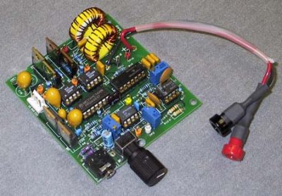
The analog pulse width modulation amplifier was designed as an integrated “blue box” approach to demonstrating the PWM process. With suitable component selection, the resulting PWM is of sufficiently high quality to demonstrate not only motor drive applications but also audio amplification. The design realizes the PWM discretely: a voltage controlled oscillator to generate the ramp, a comparator, dead-time logic, and a full H bridge to drive the load. To simplify the gate drive circuitry, each gate is driven directly from the input bus. In practice this limits the bus voltage to the maximum Vgs of the FET – about 20V; sufficient to drive a small 8Ω speaker. Test points are provided to allow investigation of every aspect of the PWM process including dead-time.
DESIGN DETAILS:
Complete design data is available. Schematic and board layout was performed using the OrCAD suite from Cadence, PSD 14.0. The design documentation is available in PDF format on this webpage.
Copyright © 2004 by Robert S. Balog, Jonathan Kimball, and Philip T. Krein.
All Rights Reserved. May be duplicated for educational use only so long as this notice remains intact.